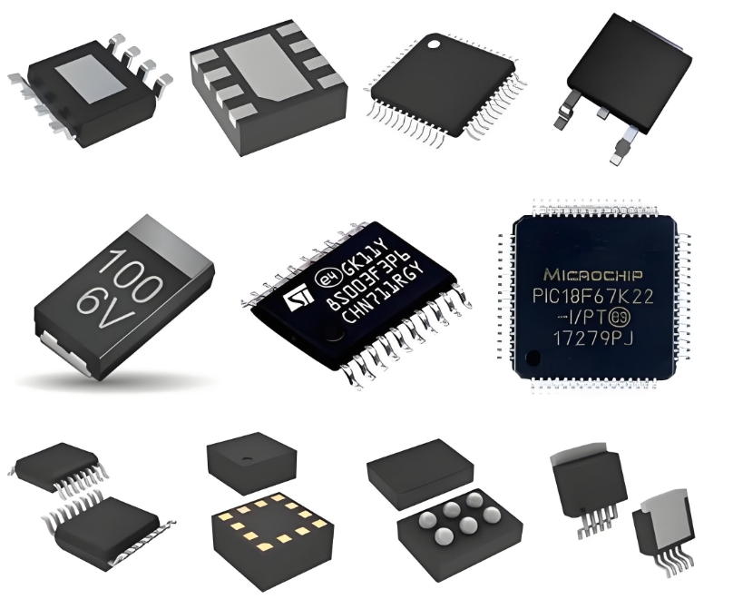
The ADL5511ACPZ from Analog Devices represents a pinnacle of monolithic, TruPwr® RMS-responding power detector technology, engineered for high-frequency applications. Its ability to accurately measure the true root mean square (RMS) power of complex waveforms makes it indispensable in modern RF systems, from cellular infrastructure to test and measurement equipment. This article delves into the sophisticated architecture of the ADL5511 and provides insights into its critical application circuit design.
**Core Architectural Principles: TruPwr® Detection**
At the heart of the ADL5511 lies its **TruPwr® detection methodology**, which is fundamentally different from simpler logarithmic amplifiers or peak detectors. Traditional detectors can be misled by high peak-to-average power ratio (PAPR) signals common in modern modulation schemes like OFDM and QAM. The ADL5511 overcomes this by computing the true RMS value of an input signal, which is directly proportional to its power regardless of the waveform's crest factor.
The internal architecture is a sophisticated cascade of functions. The input signal first passes through a **wideband linear-in-dB variable gain amplifier (VGA)**. This stage conditions the signal over a wide dynamic range. The core computation is performed by an analog computational block that effectively squares the input signal, averages it, and then takes the square root of the result. This process, **the direct mathematical calculation of RMS**, ensures exceptional accuracy even with multi-tone and digitally modulated signals. The device operates over a remarkably broad frequency range from 1 MHz to 4 GHz and a dynamic range of up to 60 dB.
**Critical Application Circuit Design Considerations**
Implementing the ADL5511ACPZ effectively requires careful attention to board-level design to preserve its high-frequency performance.

1. **Input Matching and Biasing:** The RF input (INPH) must be properly matched to 50 Ω to minimize return loss and ensure accurate power measurement. This typically involves a matching network. Furthermore, the input is internally DC-biased at approximately 1.8 V, necessitating the use of an AC-coupling capacitor (e.g., 100 pF) to block any external DC voltage. A shunt inductor to ground is often used to provide a DC path while acting as an RF choke.
2. **Power Supply Decoupling:** As with any high-speed analog IC, **robust power supply decoupling is paramount**. A combination of a 100 pF capacitor placed extremely close to the supply pin and a larger 0.1 µF capacitor is essential to filter high and low-frequency noise, preventing unwanted supply ripple from affecting the output measurement.
3. **Output Filtering and Interface:** The output (VOUT) is a DC voltage proportional to the RMS power of the input signal. A simple RC low-pass filter is recommended at the output to suppress any residual RF or switching noise. The value of the filter capacitor (e.g., 100 pF to 0.1 µF) will determine the output response time and ripple. For interfacing with an ADC, the output scaling must be considered based on the transfer function provided in the datasheet.
4. **Grounding and Layout:** A **continuous, low-impedance ground plane** is critical for stable operation. The exposed paddle (ACPZ package) must be soldered directly to the PCB ground plane to provide both electrical grounding and effective thermal dissipation. Signal traces, especially the RF input, should be kept short and direct, using controlled impedance microstrip lines where possible.
**Typical Application: Automatic Gain Control (AGC) Loop**
A primary application for the ADL5511 is within an AGC loop. In this configuration, the detector's output voltage is compared to a stable reference voltage representing the desired output power level. The resulting error signal is integrated and fed back to control the gain of a VGA or variable attenuator preceding the detector. This closed-loop system actively maintains a constant output power level, compensating for variations in input signal strength or temperature, which is crucial for transmitter chain stability.
ICGOOODFIND: The ADL5511ACPZ stands out as a superior solution for true RMS power detection due to its innovative TruPwr® architecture, which ensures accuracy with complex modulated signals. Successful implementation hinges on meticulous RF circuit design practices, including proper input matching, exceptional power supply decoupling, and a solid RF-grade PCB layout. Its primary role in AGC loops is fundamental to maintaining signal integrity in modern wireless communication systems.
**Keywords:** RMS Power Detector, TruPwr Architecture, RF Design, AGC Loop, High Frequency Modulation
